) free-standing GaN substrates
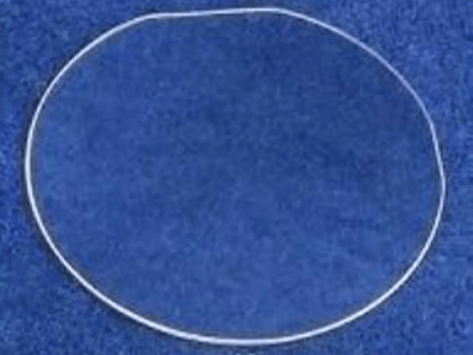
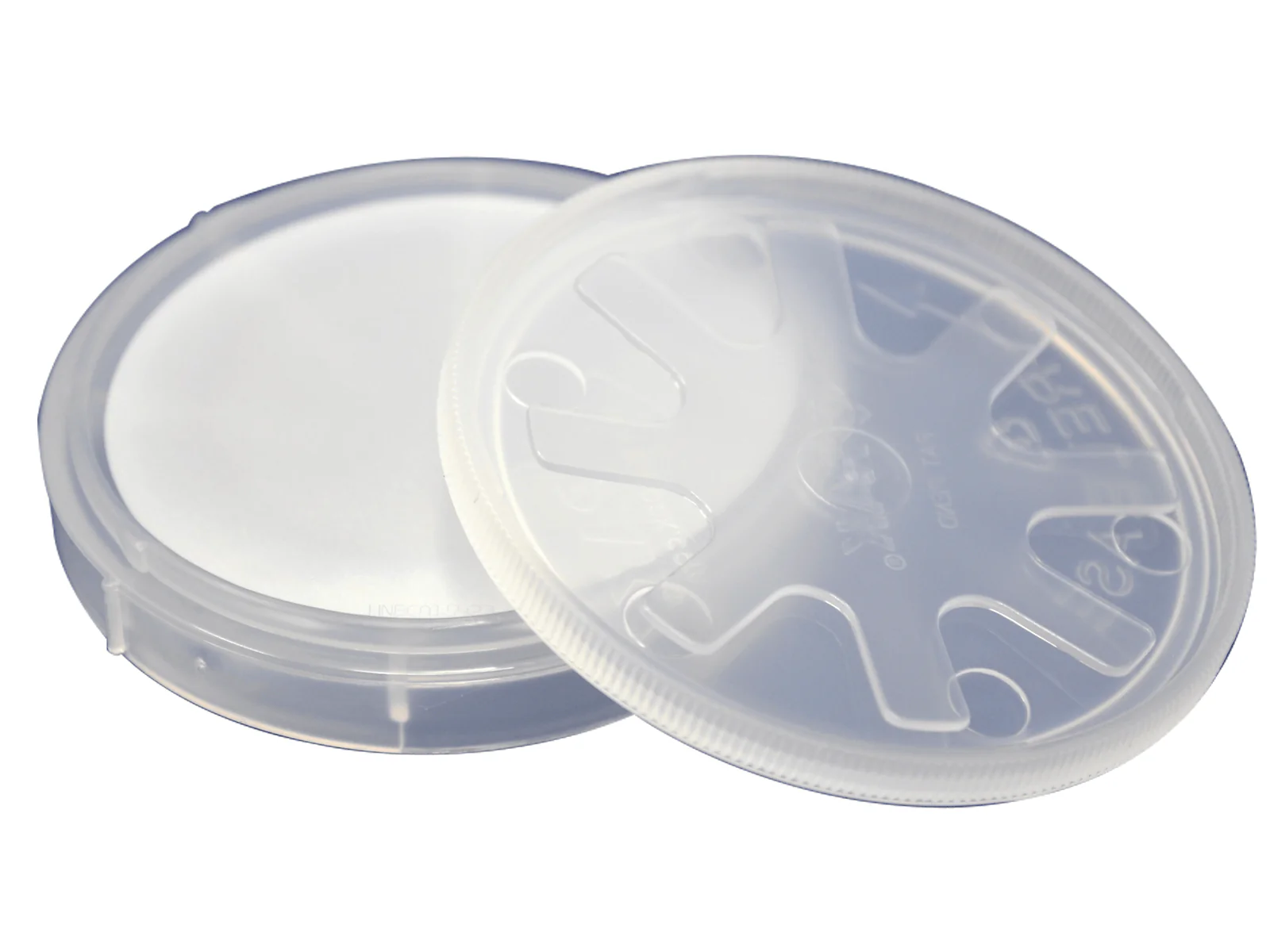
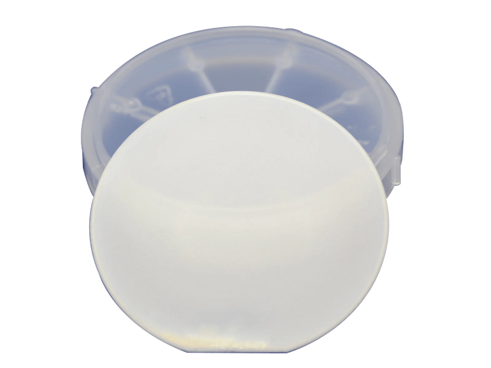
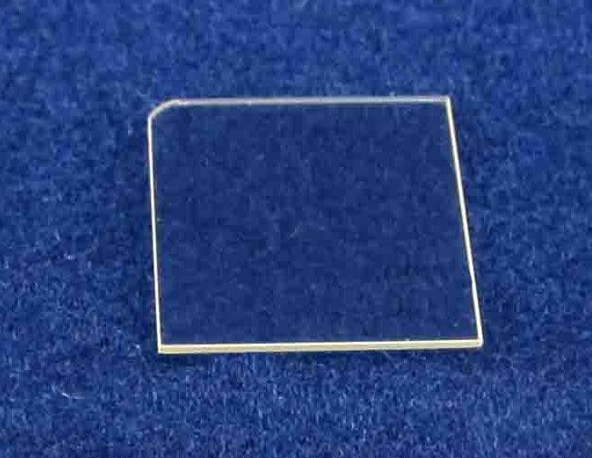
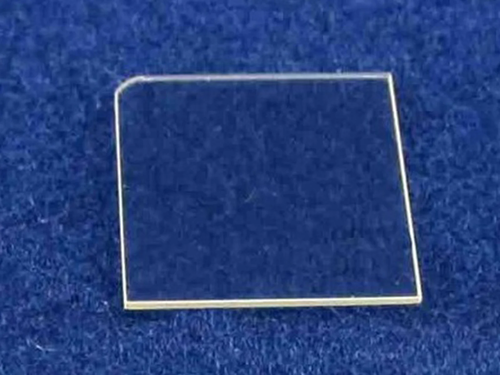
Free-standing GaN substrate, C plane (0001), semi-insulating, size 2 inch Diameter
Conductivity type: semi-insulating, Single side polish
Doping: Fe-doped (iron doping)
Please contact us for discounted rates when you order a larger quantity.
- Dimension: 2 inch, or 50.8 mm
- Thickness: 350 +/- 25 um
- Usable area: >90%
- Orientation: C-plane (0001) off angle toward M-axis <1-100> 0.35 deg+/- 0.15 deg
- Total Thickness Variation: <15 um
- Bow: <20 um
- Resistivity (300K): > 10^6 Ohm-cm
- Fe-doping concentration: ~ 3 × 1018 cm−3
-
Dislocation Density: < 9 x 105 cm-2
- Polishing: Front surface: Ra <0.5 nm, epi-ready, double side polished available per request
- Package: packaged in a class 100 clean room environment, in single wafer container, under nitrogen atmosphere.
Related Reference
1. Blue InGaN/GaN laser diodes grown on (33 ) free-standing GaN substrates
https://doi.org/10.1002/pssc.201001012
2.Review: InGaN-BASED LASER DIODES